AM Technical Solutions (AM) recently completed work on a major cleanroom construction project at a university in the Southwestern United States.
We partnered with a large semiconductor capital equipment manufacturer that produces advanced process and metrology equipment. This equipment is critical for manufacturing semiconductor (integrated circuit) chips in electronics, displays, smartphones, televisions, and solar products.
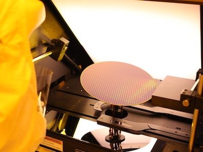
The company recently developed new capital equipment ready for 300mm wafer research. They created a new agreement with a major research university to use part of a large 300mm wafer processing cleanroom that was previously designed by our company for other large substrate processing.
The university and the capital equipment supplier called on our company to design the reconfiguration of the cleanroom and utilities, as well as tool installation designs to serve the new process equipment.
AM Delivers Tool Configuration and Other Services
A critical element of the project design was to allow for research flexibility and tool configuration changes in the future. One of the primary challenges meeting this need was determining which of the hazardous process gas distribution and abatement systems could be re-used for the new research tools, which could be shared with other users, and which needed to be replaced.
Additionally, we assisted the customer with the new installation to ensure compliance with the latest building codes in the municipality as well as adhering to university guidelines.
Our Engineering Manager led the architecture and engineering team, working closely with the equipment supplier as the requirements for the research tools evolved.
We also provided critical design support. Utilizing our extensive tool hookup experience, AutoCAD files of the older fab building, and surveys of as-built conditions, we ensured that the installation of the tools was supported by accurate architectural, structural, mechanical, electrical, and process piping designs.
Additional Challenges of the Cleanroom Construction Project
Close coordination was required with the university to verify that the tools fit in the fab and allowed subfab space. We also needed to meet the requirements from the university and tool manufacturer for clearance and maintenance access.
The AM team, with support of the customer and the university, also successfully utilized a new municipal permitting system, verifying the entire project design complied fully with the latest local code requirements.
“We appreciated the challenge presented by this project. Our team was up for the task aligning resources, plans, and prior experience with the needs of the customer and the university to reconfigure the cleanroom, deliver tool installation, and provide other cleanroom construction services,” says Sandeep Davé, AM Chief Business Officer. “We look forward to seeing how advanced semiconductor manufacturing and research flourishes in the reconfigured cleanroom environment.”
– Find out more about our capabilities supporting semiconductor projects in our Portfolio.
– Contact us today to discuss your next semiconductor construction project.

