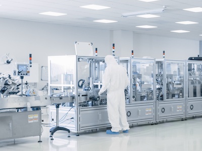
AM Technical Solutions (AM) has developed specific expertise in design build projects for semiconductor manufacturing facilities. We leverage the capabilities of our Architecture & Engineer (A&E) design team in Arizona with our Build team to provide effective solutions for our clients’ design build projects.
When customers approach us with complex, multi-phase projects that require a right-size solution, they can rely on our company to create the best strategy for the project. We will also follow through with first-time-right execution of the strategy. Our semiconductor operations experience informs our approach, strategy, and execution to drive superior value for customers.
We are currently applying our proven approach to a two-phase semiconductor lab expansion project for one of our customers. The company is looking to expand capacity and add new capabilities at their U.S. facility. Our history of supporting semiconductor tool install design and construction will successfully bring this project to completion.
Project Scope for Semiconductor Tool Install & Facility Upgrades
The scope of work for this project includes a new lab expansion and remodel of an existing lab. The estimated remodel space will cover approximately 5,000 SF of facility space. AM was contracted to provide the following services as part of the project:
- Standard design build services.
- Construction documents, construction cost, and schedule updates that will be reviewed at scheduled intervals.
- Prepare document submittal packages for permitting that will allow the work to be performed.
- Construction set that will be utilized for the post-design construction work.
- Basebuild, fit-up, and tool hookup design.
The design phase is now complete. During the first phase, our team worked to complete as-built conditions. We also needed to evaluate multiple locations for a new electrical room to ensure that all project requirements could be met.
The AM team is now working on the second phase of the project (demo and construction work). One of our primary challenges during this phase will be identifying all utilities and factory impacts associated with the demo project.
This two-phase, multi-year project will require multiple experts to lead the project. We are providing the necessary skills and subject matter experts to ensure we deliver on the time, cost, and quality requirements for our customer. We are also leveraging our connections with the trades to satisfy individual project requirements.
The AM team for this project includes an operations executive leader, a senior architect, an engineering manager, and other high-tech construction experts.
“We look forward to providing our customer with new cleanroom space to expand into,” says Robert Logston, SVP, Construction. “Our deep industry connections, extensive experience with design build construction projects, and robust semiconductor tool install capabilities will ensure that our customer is equipped with a state-of-the-art facility to support their production needs.”
– Find out more about our capabilities to deliver high-tech construction services for semiconductor facilities.
– View our portfolio of award-winning high-tech construction projects in the semiconductor industry.
– Does your company require support for a facility expansion project that includes tool install and other upgrades? Contact us today to discuss your project requirements.

