The U.S. semiconductor market is rapidly growing thanks to significant capital infusions under the CHIPS Act. As new facilities are built, companies need follow-up design support to expand capacity and continue to meet CHIPS requirements.
At AM Technical Solutions (AM), we bring decades of experience in semiconductor facility design projects to our clients. We are currently supporting a leading semiconductor company with the second phase of plans for their wafer manufacturing facility.
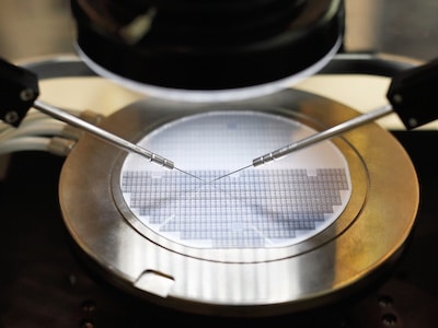
Find out how we are implementing a structured execution approach to help our client satisfy project timelines, stay within budget, eliminate rework, and continue to operate with minimal disruption during the expansion project.
Our Scope for the Semiconductor Wafer Manufacturing Design
Our client recently completed the Phase 1 build-out of a manufacturing facility on their campus. Now, we are supporting Phase 2 of the project, which involves the fit-out of a previously constructed shell space.
The fit-out will include architectural build-out, HVAC and utility system extensions, tool-integration infrastructure, and life safety provisions. This effort represents a critical compliance milestone in support of CHIPS funding requirements.
Our team will provide the following project scope to help our client maintain a state-of-the-art wafer manufacturing environment, enabling them to maintain eligibility and align with federal program timelines:
- Comprehensive coordination with project teams
- Facility system extensions
- Tool utility integration
- Permitting support
- Final construction documentation
To ensure alignment among stakeholders, we will start with a dedicated scope-alignment period. These sessions will include on-site meetings with system owners, operational staff, and tool installation teams. We will finalize the Tool Utility Matrix (TUM), confirm system strategies/sizing, and produce a Basis of Design (BOD) to guide the remainder of the design process.
Following the alignment phase, we will lead a fully integrated, multidisciplinary design effort to bring the project to 100% preparedness for construction. Our approach will incorporate QA/QC best practices, model-based coordination, stakeholder engagement, and a permitting/code compliance strategy that complies with industry standards.
We will leverage our team’s deep technical expertise in cleanroom and wafer fab environments to ensure our recommended designs meet strict performance requirements. Also, through our seamless tool integration capabilities, we will validate that the infrastructure is extended correctly, routed, and ready for the installation of critical manufacturing tools.
“We appreciate that our client has trusted us to establish a clear design baseline for the facility,” says Sandeep Davé, AM Chief Business Officer. “We are confident that our proven approach to coordinate efforts across all trades, minimize conflicts, and accelerate construction will provide our client with an innovative manufacturing facility.”
– Find out more about our capabilities to support high-tech construction projects in the semiconductor industry.
– View our portfolio of award-winning semiconductor projects.
– Does your company need support with a semiconductor manufacturing facility design project? Contact us today to discuss your latest requirements.