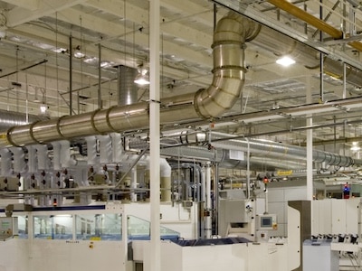
The development of cutting-edge semiconductor fabrication facilities requires precise planning and expert guidance. AM Technical Solutions (AM) brings over 30 years of experience in semiconductor design and high-tech construction services to support complex projects.
In our latest project, we are partnering with a client in Asia to develop a fully integrated compound semiconductor fab. Currently in the site evaluation and development phase, the company has engaged our team for expert support in semiconductor fab design and construction consulting to inform critical decisions on site selection and funding applications.
This international project highlights our ability to guide ambitious initiatives to successful completion. Learn how we will ensure that all three project essentials – cost, quality, and schedule – are satisfied through our collaborative approach.
How We’re Supporting a World-Class Semiconductor Fab Design
This ambitious project involves the development of a fully integrated compound device fab, which requires meticulous planning, cost management, and industry expertise. Our role will involve providing a range of consulting services designed to support strategic planning, help secure government funding, and guide the overall design and construction process.
One of our primary responsibilities is to assist in the preparation of the conceptual design of the facility with cost and schedule estimates for submission to the relevant stakeholders.
To highlight the project’s significance, we will provide high-level employee support, including principals, engineers, architects, and technical leadership. Our team’s experience with global projects will ensure that our client achieves a cost-effective and efficient design. We offer a unique perspective that considers not only capital expenditure (CapEx) but also operational expenditure (OpEx) to create a sustainable fab design.
With the project still in the early stages, careful planning is essential to ensure long-term success. We will develop a high-level schedule and planning sequence, aligned with the key deliverables and milestones the client needs to move forward.
Delivering Timely Client Support to Ensure Project Success
To support our client’s team on the ground, we will host workshops to advise on innovative construction approaches, ensuring the fab’s build is grounded in operational best practices. Topics in these workshops will include construction sequencing and insights into effective foundry operations.
To further enhance collaboration, our team will work closely with the client through regular online meetings to ensure alignment and timely exchange of vital project information. The customer will provide critical details such as wafer capacity, equipment lists, site details, device process requirements, and more information. This approach guarantees every aspect of the fab is taken into account – from utility services to staffing to operational requirements.
Overall, this project exemplifies our commitment to the future of semiconductor manufacturing. By applying our comprehensive knowledge and proven methodology, we are poised to deliver an exceptional fab design and construction solution.
“Our trusted background in the semiconductor industry allows us to provide unmatched guidance at every step of the process,” says Sandeep Davé, AM Chief Business Officer. “Because we operate with a ‘first-time-right’ focus, we ensure excellent customer outcomes every time. We look forward to helping our client bring this world-class compound device fab from conception to reality.”
– Find out more about our capabilities to support global semiconductor fabrication facility projects.
– View our portfolio of award-winning semiconductor projects.
– Does your company need support with a semiconductor fab design project? Contact us today to discuss our high-tech construction services.