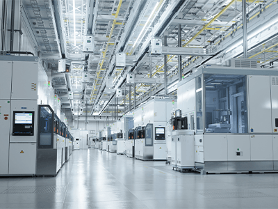
The global semiconductor industry is facing increased demand, creating a critical need to increase manufacturing capacity. Many companies are striving for optimum utilization of their existing facilities, including modifying them to meet different technology needs.
AM Technical Solutions (AM) has conducted numerous high-tech construction projects for internationally-recognized companies. We are well-positioned to support semiconductor retrofit projects by identifying and providing the best solution for our customers.
One of our clients faced the challenge of needing to retrofit an existing semiconductor facility that was designed for a different product and technology. The objective was to convert the facility to meet a different technology node.
Due to our expertise in the semiconductor industry, we were requested to assess the current facility for the company’s specified expansion scenarios and determine the effort necessary to achieve the project goals.
Our Project Scope Supporting the Semiconductor Retrofit Project
At the outset of the project, the company had several technology and product mix scenarios. Each scenario would require significant design and retrofit efforts. We leveraged our design and construction management expertise to provide our customer with estimates of the time and cost requirements to achieve the project objectives.
Due to the complex nature of semiconductor fabs, experience in every aspect of the fab is important, including design, construction, and operation. We were able to bring all these elements to our project deliverables to help the customer meet the challenge head-on.
For this specific project, we were asked to provide the following services:
- Survey the current facility
- Assess the functional fit for their future needs
- Determine which aspects need to be retrofitted
- Estimate the time and cost for the retrofit
To support this effort, we provided a highly-skilled design and construction Manager, as well as Subject Matter Experts (SMEs) for Mechanical, Electrical, and Process requirements.
For this project, we defined success as upholding our values of doing what’s right by our customer. Specifically, our goal was to deliver on all three of Cost, Schedule, and Quality (not picking two), as defined by a collaborative relationship with our customer.
“By providing our customer with a solution that fit their situation, we were able to help the company confidently move into the next step of establishing a facility that was fit for purpose,” says Sandeep Davé, Chief Business Officer. “We always strive to bring value to our customers, people, and company through a First Time Right approach, and this project was no exception.”
– Learn more about our capabilities to execute high-tech construction projects for semiconductor facilities.
– View our portfolio of award-winning high-tech construction projects.– Need support with a semiconductor retrofit project to maximize production capabilities? Contact us today to discuss your project needs.

