AM Technical Solutions (AM) has built a reputation in the high-tech industry for helping turn existing spaces into advanced semiconductor facilities without impacting running operations. We are currently supporting a leading semiconductor testing company with critical design work for their campus in the Southwestern U.S.
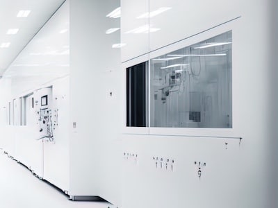
Our client is renovating a significant amount of existing area in a large semiconductor fabrication building. Included in the renovations will be new Class 1,000 and 10,000 Cleanroom areas for new tool sets, supporting equipment, and infrastructure areas. There will also be a dedicated gowning room, clean circulation to all new cleanrooms, and newly identified server rooms.
The project scope for the test floor buildout design will be spread across multiple phases, without interruptions to operations, reflecting the complexity of the work. Learn how we plan to support our client’s project goals of expanding manufacturing capabilities within their required timeline.
Our Project Scope for the Advanced Semiconductor Facility
Our team will lead a five-phase design and execution program – from schematic design through construction administration. We plan to deliver code-compliant cleanroom and test floor areas, integrate new tools and utilities into existing systems, and manage all permitting, bidding, and change control processes in close coordination with our client and additional teams:
- Phase 1: Document existing conditions, confirm codes and standards, and establish preliminary layouts and capacities for the renovated cleanroom and support areas.
- Phase 2: Turn client-approved concepts into coordinated architectural, structural, mechanical, electrical, controls, and fire protection documents for permitting and pricing.
- Phase 3: Define cleanroom, test floor, and infrastructure scope, including complete drawings, specifications, and calculations for submission to authorities and contractors.
- Phase 4: Support bidding and permitting to incorporate all required clarifications.
- Phase 5: Collaborate with our client and the contractor in the field to attend meetings, perform site observations, manage punch lists, and deliver final documents.
We organized the phased design approach to align with our client’s schedule and manufacturing objectives. Each phase builds on the previous one, progressively adding detail and certainty around cleanroom performance, utility capacities, and integration with existing systems. This approach will enable the early identification of field conditions and risks while keeping the project on track for permitting, bidding, and construction.
A multidisciplinary team will support the effort, including employees and subject matter experts (SMEs) in architectural, structural, mechanical/HVAC, electrical, controls and instrumentation, fire protection, and life safety. Throughout the project, we will work hand-in-hand with stakeholders to validate requirements and align the design with production needs.
During permitting, bidding, and construction, our team will stay closely engaged with the selected contractor and the authorities having jurisdiction. We will respond to RFIs, review submittals, participate in regular coordination meetings, and provide field observations and reports to help maintain quality and compliance.
Our standardized practices will ensure that our client can make timely, well-informed decisions while maintaining control over scope and project risk.
“We appreciate the opportunity to guide the direction of this advanced testing facility through our integrated design approach,” says Dan Codi, AM Chief Operating Officer. “Our goal is to deliver an advanced semiconductor facility that expands cleanroom capacity, integrates seamlessly with existing infrastructure, and positions our client for scalable manufacturing growth.”
– Find out more about our capabilities to support high-tech construction projects in the semiconductor industry.
– View our portfolio of award-winning semiconductor projects.
– Does your company need support converting existing space into advanced semiconductor facilities? Contact us today to discuss our capabilities.