Semiconductor

Inside look at the hallway of a semiconductor facility

Providing Senior Construction Management Services for a Global Semiconductor Project

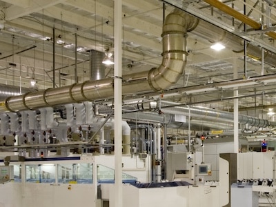
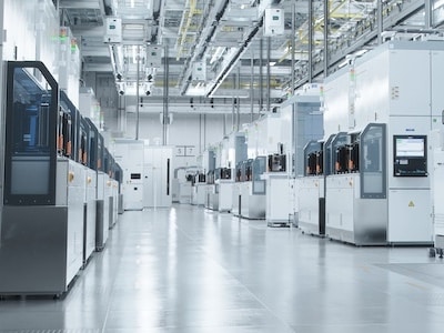
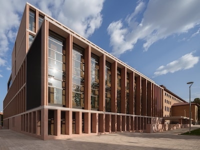
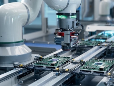
AM Technical Solutions (AM) is a proven high-tech construction firm capable of providing senior construction management services for complex projects across the globe. We were recently awarded scope for an international semiconductor project that will help the end user achieve significant advancements in manufacturing capability to positively impact their country’s economy. Our Architectural and Engineering […]

Providing Senior Construction Management Services for a Global Semiconductor Project Read More »

Close-up view of a manufactured aerospace part

Providing Architecture and Engineering Support for An Aerospace Semiconductor Facility

Throughout the history of AM Technical Solutions (AM), we have supported leading companies in the aerospace and defense industry by providing consulting services for semiconductor facility design projects. We are currently providing a global aerospace company with Architecture and Engineering services that will span multiple projects. We will lend our expertise to support the production

Providing Architecture and Engineering Support for An Aerospace Semiconductor Facility Read More »

Poster for the 4th Annual Global Chamber® Semiconductor Summit held February 2025 in Phoenix, Arizona

Participating in the 4th Annual Global Chamber® Semiconductor Summit

The semiconductor industry is at the heart of technological innovation and capital investments across the globe. With its growth comes immense complexity, challenges, and opportunities. This is why the 4th Annual Global Chamber® Semiconductor Summit, held February 19-20, 2025, in Phoenix, Arizona, was a focal point for industry leaders. AM Technical Solutions (AM) was proud

Participating in the 4th Annual Global Chamber® Semiconductor Summit Read More »

Inside of a semiconductor facility

Enhancing Semiconductor Fab Design with Expert Consulting

The development of cutting-edge semiconductor fabrication facilities requires precise planning and expert guidance. AM Technical Solutions (AM) brings over 30 years of experience in semiconductor design and high-tech construction services to support complex projects. In our latest project, we are partnering with a client in Asia to develop a fully integrated compound semiconductor fab. Currently

Enhancing Semiconductor Fab Design with Expert Consulting Read More »

Inside of a semiconductor facility

Master Planning and Design Services for a Chiller Replacement Project

AM Technical Solutions (AM) has built a highly capable roster of experts to handle the most complex semiconductor projects. One such project required the full cooperation of multiple teams to execute a capital project for a large semiconductor company. Our client is being required to replace multiple water-cooled centrifugal chillers in phases to prevent disruptions

Master Planning and Design Services for a Chiller Replacement Project Read More »

Semiconductor chip held by a mechanical instrument

Providing Semiconductor Construction Expertise for a Capital Project in India

The global semiconductor industry is undergoing rapid changes, with new opportunities emerging in countries like India that currently do not have volume semiconductor manufacturing capacity. AM Technical Solutions (AM) is playing a critical role by supporting the engineering, design, and construction of a new semiconductor facility in this emerging market. The project signals a major

Providing Semiconductor Construction Expertise for a Capital Project in India Read More »

Exterior of a university research building

Providing Cleanroom Expertise for an Innovative University Project

AM Technical Solutions (AM) appreciates the opportunity to support the educational sector throughout North America. We believe there is tremendous value in providing high-tech construction services to support the advancement of research in various fields. We were recently awarded a cleanroom consulting project in Western Canada to ​​assist with the Design, Construction, Commissioning, and Certification

Providing Cleanroom Expertise for an Innovative University Project Read More »

Semiconductor facility assembly

Supporting an Assembly and Test Semiconductor Facility Project in India

Earlier this year, AM Technical Solutions (AM) announced our first major semiconductor project in India. Now, we are embarking on another significant project that will help transform the country’s semiconductor market. We were recently awarded a design scope for a Semiconductor Assembly and Test facility project in India. Learn how we plan to apply our

Supporting an Assembly and Test Semiconductor Facility Project in India Read More »

Inside a semiconductor cleanroom facility

Converting an Existing Space into a Semiconductor Cleanroom Facility

AM Technical Solutions (AM) is known throughout the semiconductor industry as a leading provider of high-tech construction services for complex and high-value projects. Our team recently completed a mechanical design and cleanroom construction project to support the expansion of a client’s facility. Our client is a global leader in semiconductor solutions for advanced wireless devices,

Converting an Existing Space into a Semiconductor Cleanroom Facility Read More »