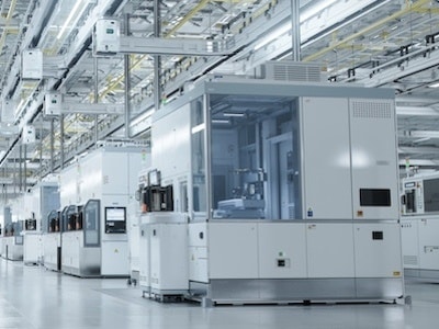
AM Technical Solutions (AM) supports the Design and Construction of highly complex high-tech construction projects with strict project requirements. We recently supported the construction of a large advanced semiconductor manufacturing facility for a Tier 1 Semiconductor company.
A critical challenge for this infrastructure project was needing to meet or exceed an aggressive delivery schedule in a dynamic working environment. Learn how our team came together to fully satisfy the construction project requirements through expert planning and agile project management.
Handling the Complexity of an Advanced Semiconductor Project
The complexity of the project stemmed from several critical requirements:
- The facility had to be planned around an existing and operating fab.
- The project and design work could not disrupt existing operations while connecting utilities and spaces to existing or expanded facility systems.
- The project work had to adhere to vibration for sensitive process equipment and meet stringent environmental standards.
Given the high stakes involved in advanced semiconductor manufacturing – where time to market can significantly influence product pricing and profitability – the project was bound by a tight schedule, cost, and quality requirements.
Our Subject Matter Experts (SMEs) included Architectural, Industrial, Electrical, Civil, and Mechanical Engineering, BIM designers, and modelers. These experts were pivotal in addressing complex design issues such as spatial planning for intricate utility routings, air flow schemes, scalability of facility systems, and compliance with building codes.
Throughout the project, numerous adjustments were necessary, particularly as changes in manufacturing processes and technology emerged. Our team’s ability to adjust to these dynamics in an agile project management style was crucial. This involved solving intricate design issues in collaboration with the customer and other firms, incorporating a new BIM software tool, and communicating with multiple design teams.
The outcome of the project was exceptionally positive. The client praised our team for going above and beyond to deliver the project scope ahead of schedule without disrupting the ongoing operations of the adjacent facility.
“The successful expansion of the semiconductor facility showcased our team’s expertise, agile management, and teamwork in advanced high-tech construction projects,” says Terry Behrens, VP of Engineering and Design. “We are proud of our team for their commitment to the project, which surpassed client expectations and enhanced our reputation for managing complex, high-stakes projects.”
– Find out more about our capabilities to support high-stakes semiconductor projects.
– View our portfolio of award-winning semiconductor projects.
– Does your company need support with an advanced semiconductor construction project? Contact us today to discuss your project needs.

