AM Technical Solutions (AM) continuously looks for opportunities to introduce new technology that can support our delivery of high-tech construction projects to clients.
The latest new technology that we are utilizing is scanning technology that will enable us to quickly identify problematic areas at the construction site and rapidly implement solutions. This effort will help us meet our promise of delivering on all three (cost, schedule, and quality) for every project, every time.
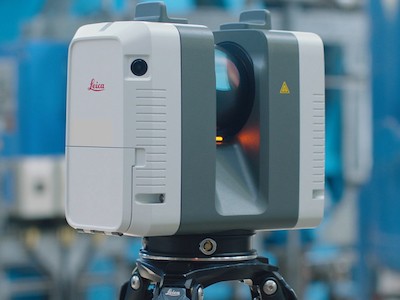
We would like to highlight one piece of scanning technology that we are planning to deploy at a construction site for a semiconductor facility. A Leica laser scanner will allow our project teams to capture changes in the construction environment and simplify complexities at the project site.
How We’re Using the Laser Scanner in High-Tech Construction
AM has contracted with one of our customers to support improvements to their semiconductor facility. We will produce scans of the subfab and provide our customer with an up-to-date status report on the building conditions during construction and buildout.
Our team of experts will be utilizing a scanning crew to facilitate continuous scanning of the sub-fab space during the project. The crew will be utilizing an RTC360 Leica laser scanner and a CAD workstation to support this effort.
The benefits of this collaborative effort include the following:
- Continuous scanning and processing dedicated to the subfab.
- Access to approximately 100-120 high-resolution scans per day to support near-real-time visibility.
- Ability to make rapid adjustments due to the scan crew working on-site with the project team to scan, process, post, share, and collaborate.
- Scans will be completed in a sequence consistent with the project schedule.
- The workflow will provide trade contractor modelers with weekly visibility into new installations as they occur in the field.
The use of this advanced laser scanning technology will help reduce the number of workers required to be in the field at the same time. This will alleviate a common challenge during construction at semiconductor facilities.
Oftentimes, these types of projects become highly congested because multiple teams work in one area at the same time trying to meet compressed schedules. Through the use of scanning technology, we will be able to perform timely scans and create clarity around how to address complex problems. The end result will be deploying the right people to the right location at the right time to address high-priority issues.
“We are eager to introduce laser scanning technology into our high-tech construction projects to create even greater value for our customers,” says Dan Codi, Chief Operating Officer. “The technology will create tremendous efficiencies and enhance our ability to deliver on all three for our customers through a ‘first-time-right’ approach.”
– Find out more about our capabilities to deliver high-tech construction services for semiconductor facilities.
– View our portfolio of award-winning high-tech construction projects in the semiconductor industry.
– Need high-tech construction services for a semiconductor facility project? Contact us today to discuss your project requirements and learn more about how we can utilize laser scanner technology at your project site.

