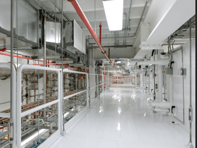
As semiconductor technology continues to advance at a rapid pace, there are greater demands placed on facilities to support technological innovation. Fortunately, AM Technical Solutions (AM) continues to lead innovation in high-tech construction project delivery to support the latest needs for our customers.
We recently engaged in a cleanroom architectural construction project for one of the leading semiconductor companies in the world. This complex project calls for our company to deliver a multitude of services to provide our customer with a world-class cleanroom facility to support the fabrication of advanced semiconductors.
The project work began in February 2021. In preparation for the construction aspect of the project, we built out an equipment list, coordinated the logistics required to bring together the various trades, managed revisions, addressed code requirements, and provided project management support.
Scope of Work for Cleanroom Architectural Construction Services
Our company was commissioned to provide critical cleanroom architectural construction services covering a tremendous amount of space estimated at 54,000 SF. The comprehensive project work includes the following:
- Install cleanroom interstitial space.
- Install Nortek Ceiling System and FFUs.
- Perform structural calculations to ensure facility integrity.
- Provide Revit design for grid system.
- Provide and install double wall system.
- Demo existing cleanroom wall.
- Furnish and install raised access floor system.
- Design underfloor air barrier.
- Design above ceiling air barrier.
- Provide BIM model coordination using AM systems.
We are confident in our ability to deliver this project on time, on budget, and of the highest quality because of our proven approach to even the most complex cleanroom construction projects.
Specifically, we self-perform all cleanroom installation with AM personnel, we have multiple long-term relationships with material providers that enables us to select the best products according to the client’s project budget and needs, and we offer the best cost solution to meet our client’s criteria with no unforeseen change orders.
Additionally, we have an internal design/engineering stamping capability and an internal NEBB Cleanroom Certification capability to ensure that the design and construction will pass certification criteria.
“We welcome the opportunity to take on multi-year, highly-involved cleanroom architectural construction projects for our clients,” says Sandeep Davé, Chief Business Officer. “We understand what it takes to deliver high-tech construction projects with a first-time-right mentality so that our clients can focus on their innovative research.”
– Find out more about our high-tech construction capabilities for semiconductor facilities.
– View our Portfolio of high-tech construction project delivery.
– Contact us today to discuss leveraging our team’s capabilities and expertise to support your next semiconductor project.

