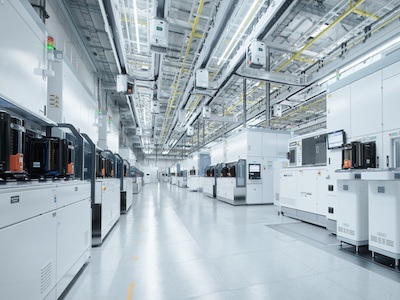
AM Technical Solutions (AM) is capable of providing high-tech design and construction expertise to semiconductor companies in a variety of ways.
We can deliver an end-to-end solution for the architecture, design, engineering, and construction of a semiconductor manufacturing facility. And, we can start at the beginning of the process by helping clients make an initial determination of how to efficiently use their space.
For example, we recently supported a leading U.S. biotechnology company with a feasibility study to help them determine the ideal path to expand manufacturing operations. We are confident that our team provided the customer with the information they needed to make an informed decision about their available options for the site configuration.
Our Project Scope for the Semiconductor Manufacturing Facility
The semiconductor company requested that we conduct a preliminary study of two options for construction at their space:
- Option 1: retrofit the current facility into an existing warehouse space to create a new fabrication facility.
- Option 2: start from scratch with a new build construction project at their existing site.
The company also requested a high-level construction schedule and a comparison of the cost per sq. ft. for each option. We executed the following plan to evaluate the current and future capabilities of their space:
– Pre-Work: Our experts reviewed documents, drawings, and site layouts provided by our customer. We sought to understand the current use of the facility and understand any constraints that could prevent the best use of the facility.
– Site Visit: We scheduled an on-site visit to the current facility to walk the site and better evaluate their utilization options:
- Reviewed current operations at the site.
- Examined the state of the facility, facility equipment, and utilities.
- Toured the warehouse, existing fab zone, and the proposed expansion areas.
- Discussed the short-term and long-term goals of the two expansion options that were being considered.
- Held other sessions to gather additional information that would be helpful for the development of the feasibility study.
– Report: After completing the site visit, we provided our customer with a thorough assessment of the two proposed areas. Our report included the following information:
- Comments on the pros and cons of the two expansion options.
- Our recommendation on the best option to hit time-to-market desires.
- A high-level review of existing utilities to support compatibility for future expansion.
- A high-level review of the structural requirements to support operations for either option.
- An estimate of the cost per sq. ft. of cleanroom space required for the options.
- An overview of the current semiconductor industry challenges and potential constraints with expansion projects.
Now that we have performed the initial assessment, we are prepared to provide our customer with BOD/conceptual design support in future phases. We can also provide necessary high-tech construction services depending on which option the company selects.
“Semiconductor companies need to make the best use of their facilities and need to modify existing spaces to meet the changing technology and capacity requirements,” says Sandeep Davé, AM Chief Business Officer. “We are eager to lend our expertise to help companies effectively maximize the capabilities of their facilities.”
– Find out more about our high-tech construction services for semiconductor companies.
– View our portfolio of award-winning high-tech construction projects for semiconductor fabrication facilities.
– Need to perform a feasibility study for your semiconductor manufacturing facility? Contact us today to discuss your goals and objectives. Let’s schedule an assessment for your company.

