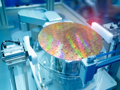
Semiconductors that can perform far better than Silicon
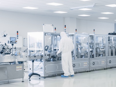
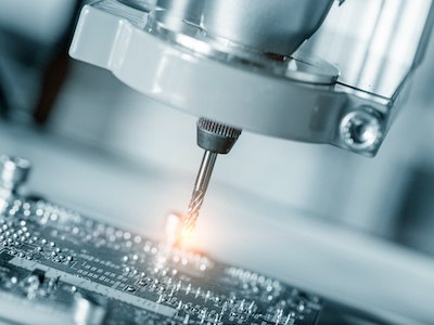
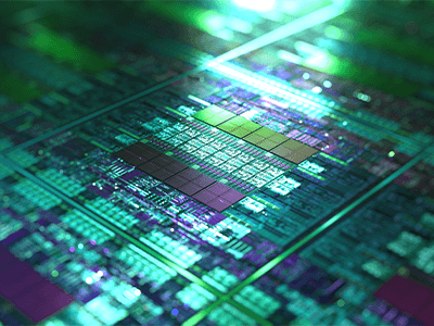
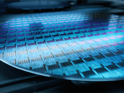
Researchers from MIT and elsewhere have found a material that can perform much better than silicon. The next step is finding practical and economic ways to manufacture it. Silicon is one of the most plentiful elements on Earth, and in its pure form, the semiconductor material has become the foundation of much of modern technology, including microelectronic […]
Semiconductors that can perform far better than Silicon Read More »