Intel Announces Next US Site with Landmark Investment in Ohio
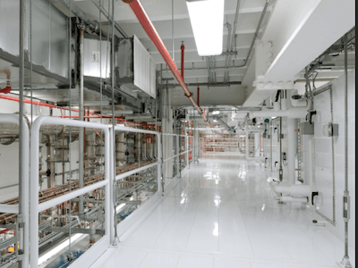
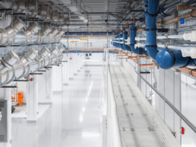
LICKING COUNTY, Ohio, Jan. 21, 2022 – Intel today announced plans for an initial investment of more than $20 billion in the construction of two new leading-edge chip factories in Ohio. The investment will help boost production to meet the surging demand for advanced semiconductors, powering a new generation of innovative products from Intel and […]
Intel Announces Next US Site with Landmark Investment in Ohio Read More »